|
|
|
|
|
|
|
|
|
|
COREMA-WT Complete system |
|
|
|
|
|
|
|
|
|
|
|
|
|
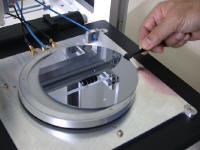
Loading a 150 mm GaAs wafer onto the pneumatic deposition ring |
|
|
|
|
|
|
|
|
|
|
|
|
|
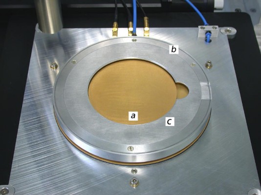
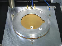
COREMA-WT pneumatic deposition ring with 100 mm adaption |
|
|
|
|
|
|
|
|
|
|
|
|
|
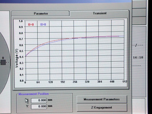
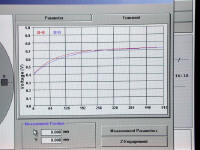
Charge transient after application of voltage step |
|
|
|
|
|
|
|
|
|
|
|
|
|
M-shaped macroscopic resistivity variation |
|
|
|
|
|
|
|
|
|
|
|
|
|
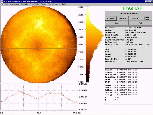
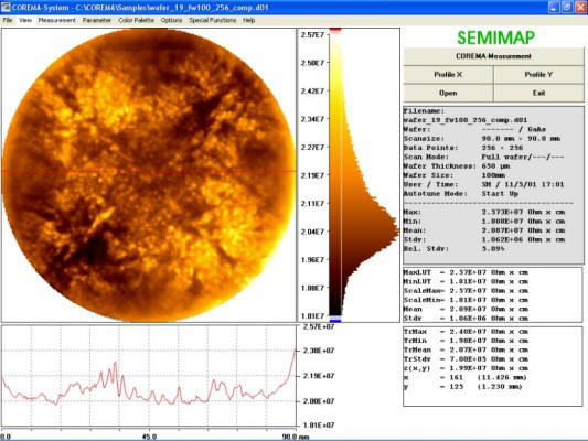
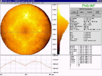
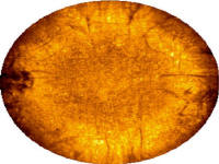
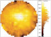
Resistivity topogram of 100 mm GaAs wafer |
|
|
|
|
|
|
|
|
|
|
|
|
|
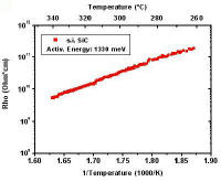
SiC temperature dependence of resistivity (Arrhenius plot) |
|
|
|
|
|
|
|

|
|
|
|
|
|
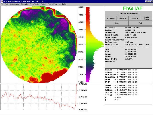
Resistivity topogram of GaAs wafer |
|
|
|
|
|
|
|
|
|
|
|
|
|
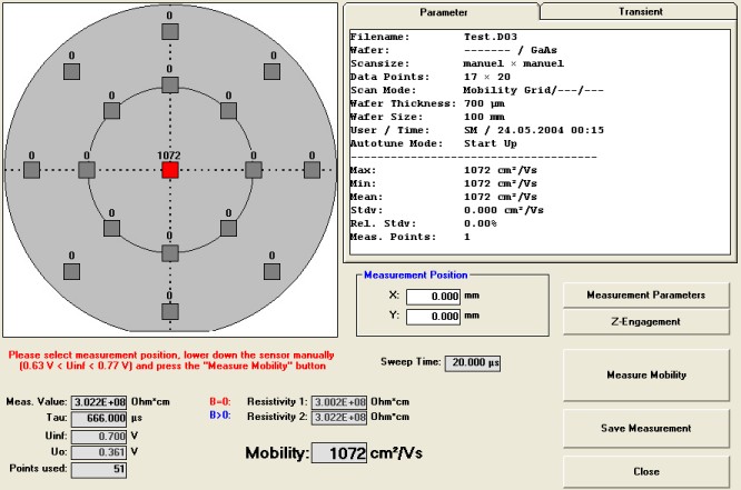
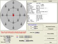
17 points measurement plan |
|
|
|
|
|
|
|
|
|
|
|
|
|
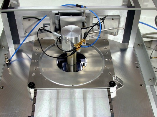
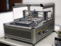
COREMA-RM system with manual translation stage |
|
|
|
|
|
|
|

|
|
|
|
|
|
COREMA-RM: detail with probe head and wafer chuck |
|
|
|
|
|
|
|
|
|
|
|
|
|
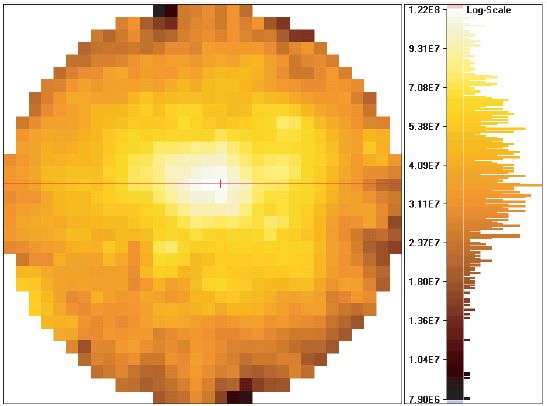
Resistivity topogram of 100 mm GaAs wafer |
|
|
|
|
|
|
|

|
|
|
|
|
|
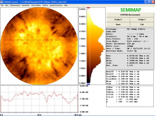
Resistivity topogram of 100 mm GaAs wafer |
|
|
|
|
|
|
|
|
|
|
|
|
|
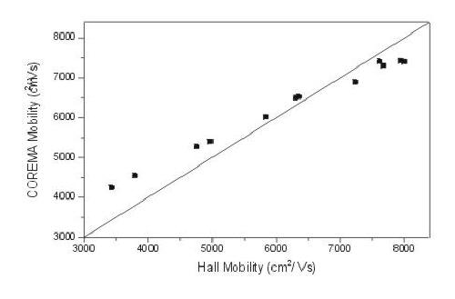
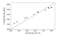
Corema mobility vs. Hall mobility |
|
|
|
|
|
|
|
|
|
|
|
|
|
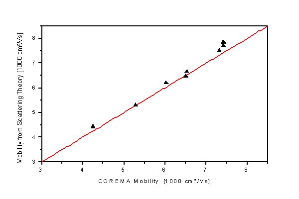
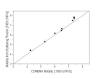
Comparison of mobility data with drift mobility obtained from ionized impurity scattering |
|
|
|
|
|
|
|
|
|
|
|
|
|
Resistivity topogram for SiC wafer with good homogeneity |
|
|
|
|
|
|
|
|
|
|
|
|
|
Resistivity topogram for SiC wafer with low resistivity inclusions |
|
|
|
|
|